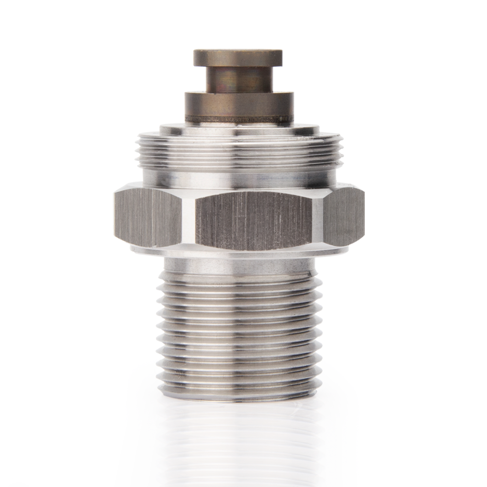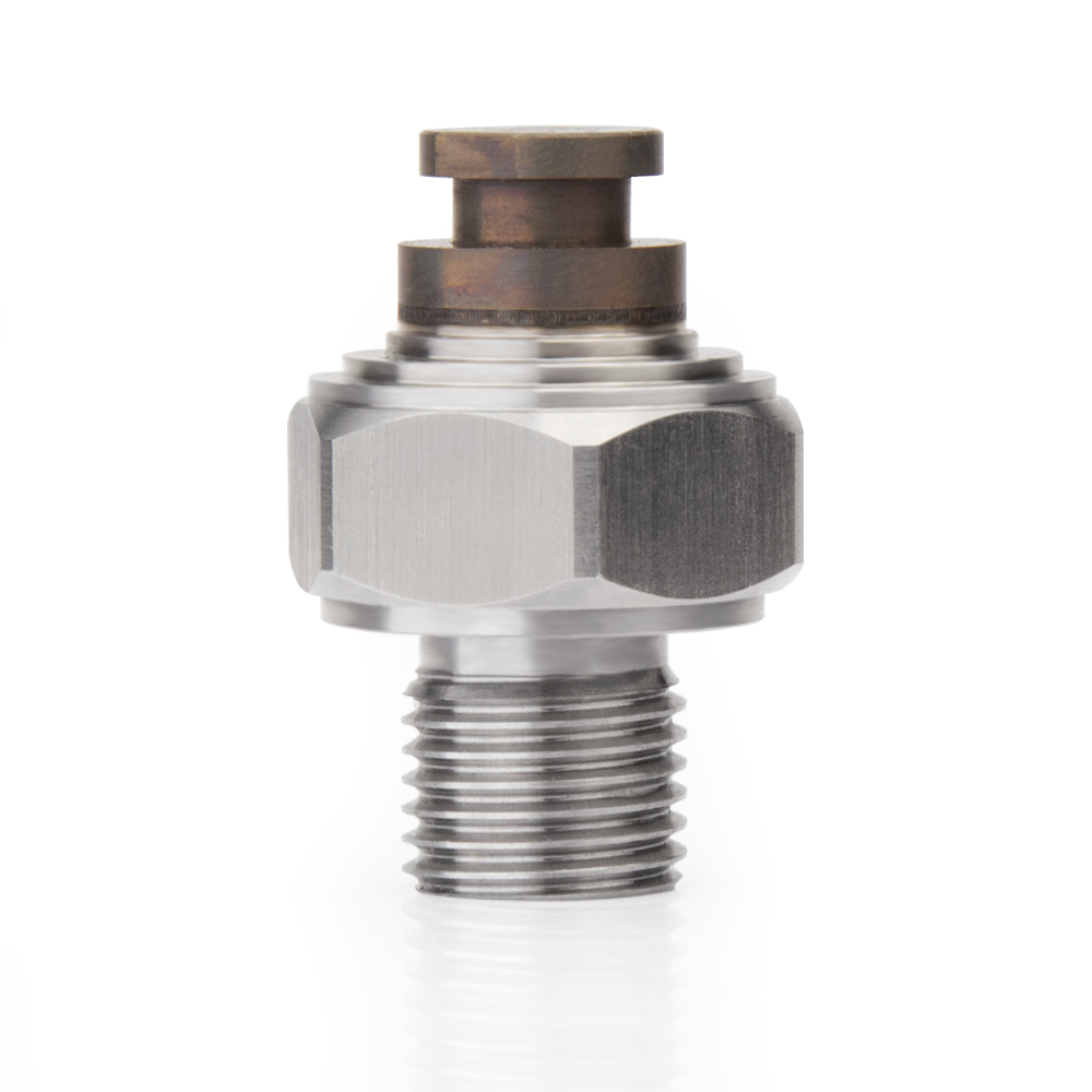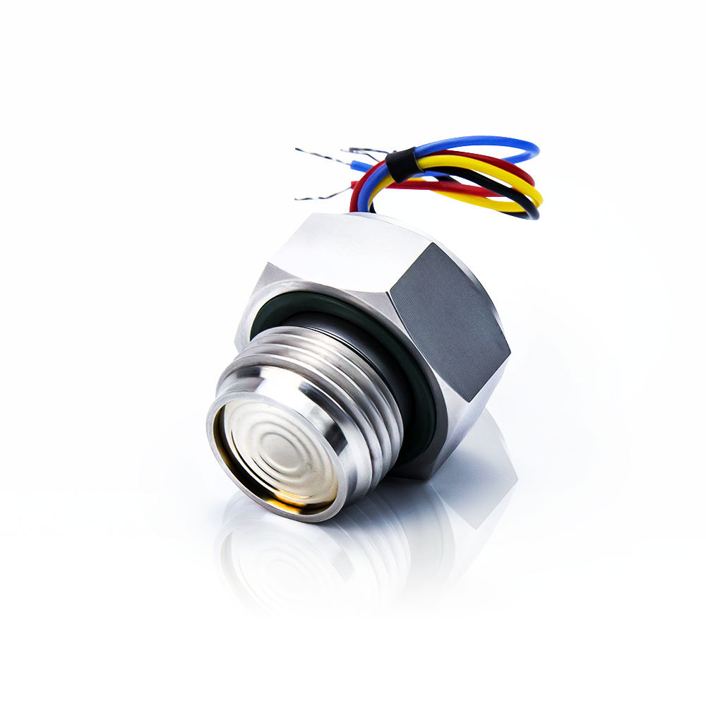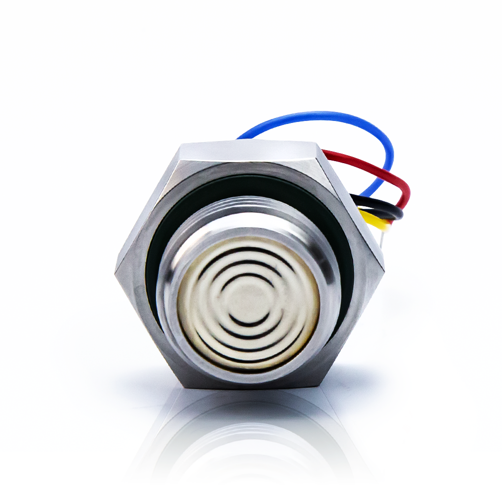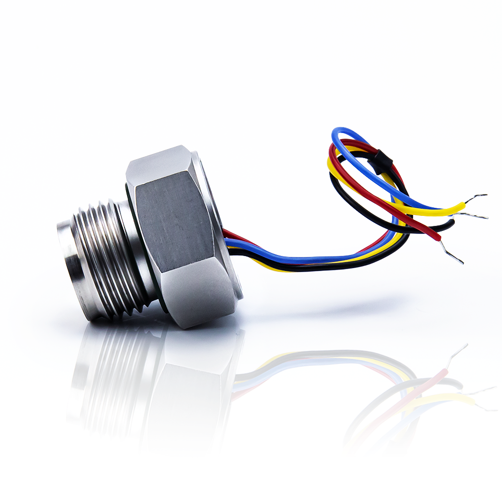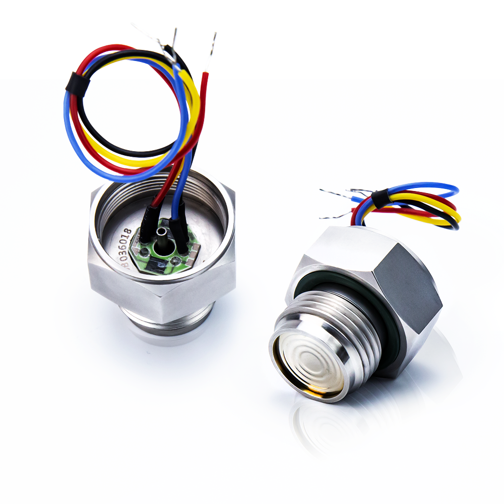
Structure condition
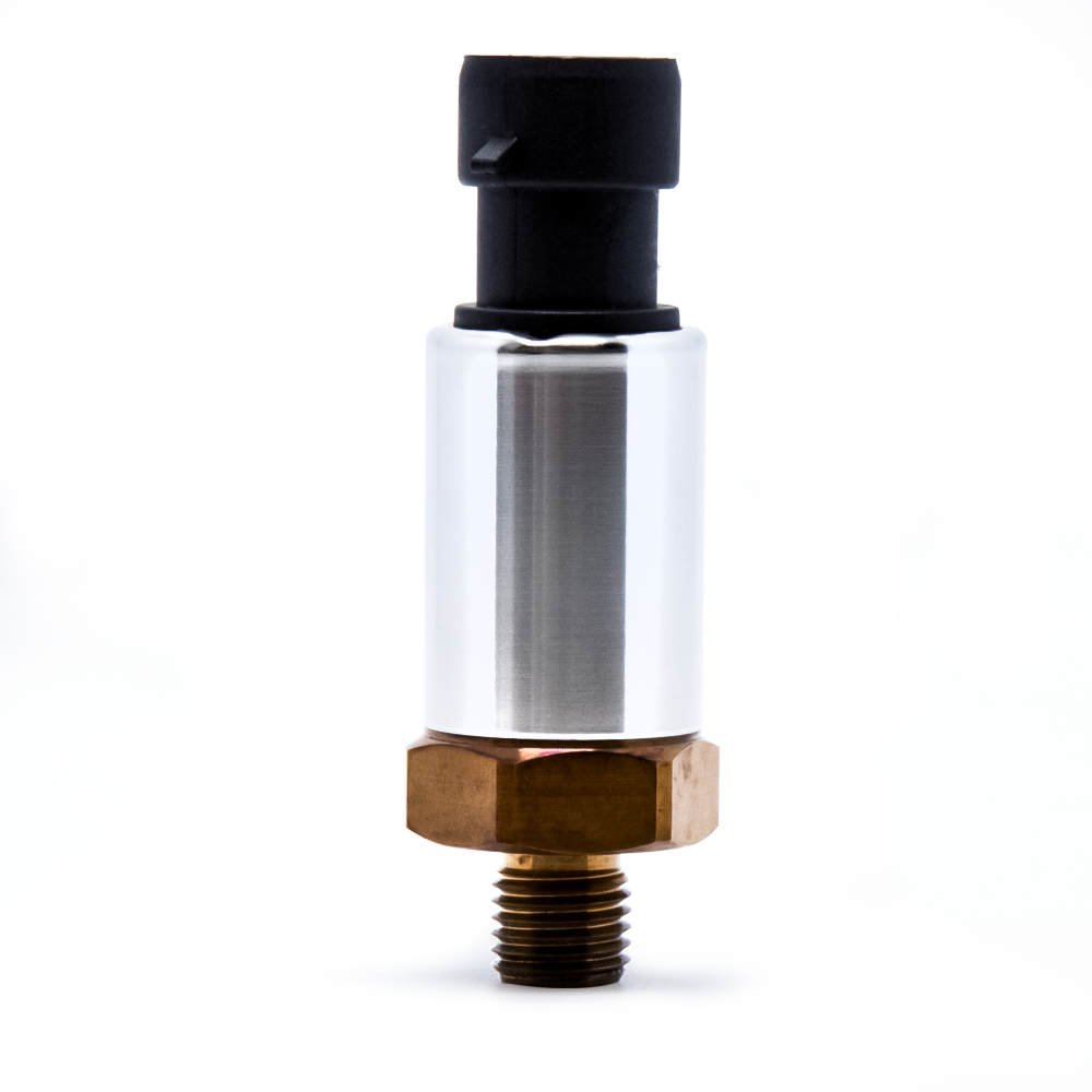
Rear thread: M24*1 Internal thread
Housing material: SS 316L
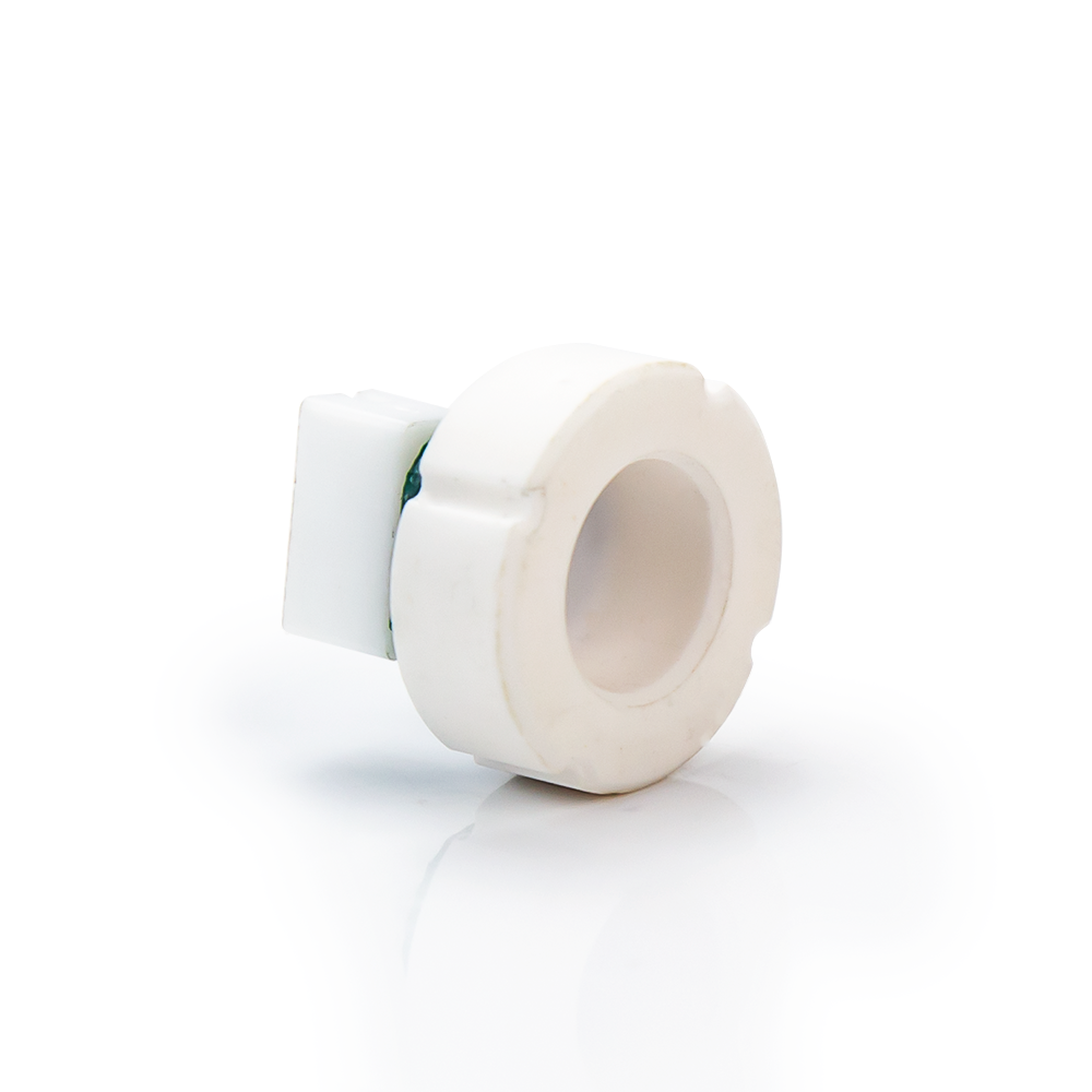
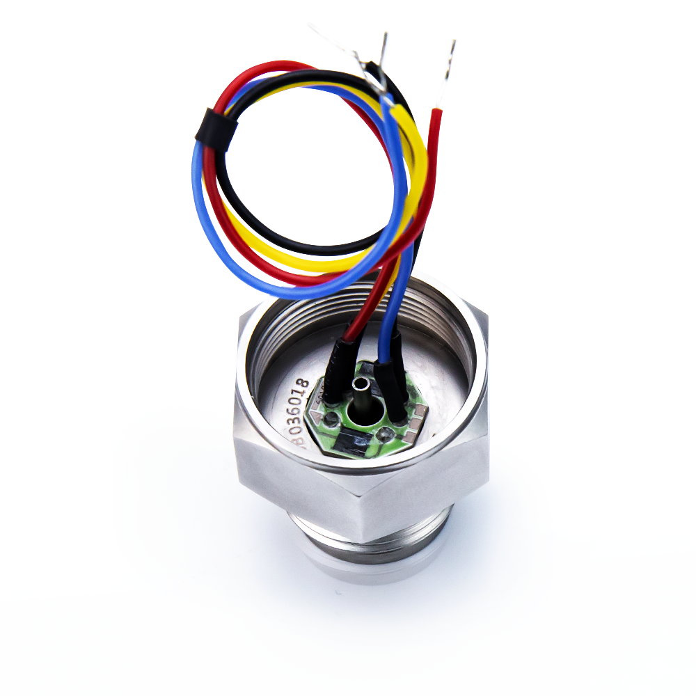
Pin Wire: Gold-plated karaf/100mm silicone rubber wire
Back pressure: tube SS 316L (gauge and negative pressure only)
Seal ring: nitrile rubber
Electrical Condition
Power supply: ≤2.0 mA DC
Impedance input: 3 kΩ ~ 6 kΩ
Impedance output: 4 kΩ ~ 6 kΩ
Response: (10%~90%):<1ms
Insulation resistance: 100MΩ,100V DC
Over pressure: 2 times FS, 5times for 0B/0A/02
Environment Condition
Media applicability: fluid which has no corrosion on stainless steel and nitrile rubber
Shock: No change at 10gRMS,(20~2000)Hz
Impact: 100g,11ms
Location effects: Deviate 90° from any direction, zero change≤±0.05%FS
Basic Condition
Environment temperature:(25±1)℃
Humidity:(50%±10%)RH
Atmospheric pressure: (86~106) KPa
Power supply:(1.5±0.0015)mA DC
All tests are in accordance with relevant national standards, including GB / T2423-2008, GB / T8170-2008, GJB150.17A-2009, etc., and also comply with the Company’s “Pressure Sensor Enterprise Standards” provisions of the relevant content.
Parameters(@1.5 mA DC)
| Item | Min. | Typ. | Max. | Units |
| Linearity | ±0.15 | ±0.2 | %FS,BFSL | |
| Repeatability | ±0.05 | ±0.075 | %FS | |
| Hysteresis | ±0.05 | ±0.075 | %FS | |
| Zero output | ±2.0 | mV DC | ||
| FS output | 45 | 130 | mV DC | |
| Compensated temp. range | 0~70(0A/0B 0~60) | ℃ | ||
| Working temp. range | -40~125 | ℃ | ||
| Storage temp. range | -55~150 | ℃ | ||
| Zero temp. error | ±0.75 | ±1.0 | %FS @ 25℃ | |
| Full temp. error | ±0.75 | ±1.0 | %FS @ 25℃ | |
| Long term stability error | ±0.1 | %FS/year |
| Note:
1. The above performance indicators are tested under the benchmark conditions. 2. The temperature range for temperature drift test is the compensation temperature range. |


| Pin | Electrical connection | Wire color |
| 4 | +IN | Black |
| 5 | -OUT | Blue |
| 11 | +OUT | Red |
| 12 | -IN | Yellow |